“Less Energy Higher Performance & Efficiency
Low-Carbon & Sustainable Growth”
AQNMOL
“Exploring Advanced Optoelectronic and Functional Devices
with Advanced Quantum- & Nano-structures and Materials”
Welcome to the Advanced Quantum-Nano Materials & Optoelectronics Laboratory (AQNMOL) !
AQNMOL is dedicated to exploring the potentials of advanced optoelectronic and functional devices and technologies that consume less energy, produce energy, offer higher performance & efficiency, i.e. photodetectors, sensors, energy generation, photovoltaics (PV) and light emitting diode (LEDs), etc. The advancement and development of energy saving & highly-efficient applications heavily reply on the improvement of novel quantum- and nano-structures and associated material systems.
AQNMOL focuses on the fabrication & characterization of advanced quantum- and nano-structures and materials & related device applications by unique Physio-Chemical approaches combining both the physical vapor deposition (PVD) of the pulsed laser deposition (PLD), sputtering, rapid thermal process (RTP) and chemical solution-based synthesis of the spin coating, electrochemical and potentiostat. Physicochemical research utilizes the advantages of both physical and chemical synthesis and fabrication and can offer advanced hybrid nanostructures and devices.
The characterizations utilize various equipment such as atomic force microscope (AFM), scanning electron microscope (SEM), energy dispersive x-ray spectroscope (EDS), Raman, photoluminescence (PL), UV-VIS spectroscopy, I-V (Photoresponse) measurements, X-ray diffraction (XRD) spectroscopy, X-ray photoelectron spectroscopy (XPS), electrochemical analysis and fabrications (CV, CA, LSV and EIS), simulations using finite-difference time domain (FDTD), Origin, Sigma plot, etc.

“The most important thing in the Olympic Games is not winning but taking part;
the important thing in life is not the triumph but the struggle,
the essential thing is not to have conquered but to have fought well.”
Pierre de Coubertin
(Founder of the International Olympic Committee)
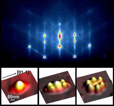

Prof. Dr. Jihoon Lee, Ph.D., MBA
Professor
Department of Electronic Engineering
Kwangwoon University
Seoul, South Korea
Email: jihoonlee@kw.ac.kr
Email: jihoonleenano@gmail.com
TEL: 82-2-940-5297
FAX: 82-2-942-5235
Address: 635 Hwado Building
Department of Electronic Engineering
Kwangwoon University
Nowon-gu Seoul 01897
South Korea
Special Issue Editor
Nanomaterials
*IF 5.719 (JCR 2021)
MDPI Basel, Switzerland
Editorial Board
Discover Nano
* IF 5.418 (JCR 2021)
Springer New York, USA
Selected Publications:
* Over 170 SCI Journal Publications:
https://orcid.org/0000-0002-0508-486X
- Dual-Functional Ru/Ni-B-P Electrocatalyst Toward Accelerated Water Electrolysis and High-Stability, Small, 2307533 (2023).
- Ni-B-P micro spheres for superior water splitting OER electrocatalyst satisfying industrial operational requirement, Chemical Engineering Journal, 462, 142177 (2023).
- Hybrid UV Photodetector Design Incorporating AuPt Alloy Hybrid Nanoparticles, ZnO Quantum Dots, and Graphene Quantum Dots, ACS Applied Materials & Interfaces, 15, 1 (2022).
- Hybrid Device Architecture Using Plasmonic Nanoparticles, Graphene Quantum Dots, and Titanium Dioxide for UV Photodetectors, ACS Applied Materials & Interfaces, 13, 2 (2021).
- Improved Photoresponse of UV Photodetectors by the Incorporation of Plasmonic Nanoparticles on GaN Through the Resonant Coupling of Localized Surface Plasmon Resonance, Nano-Micro Letter, 12, 91 (2020).
- Enhanced Spatial Light Confinement of All Inorganic Perovskite Photodetectors Based on Hybrid Plasmonic Nanostructures, Small, 2004234 (2020).
- Self‑Assembled Al Nanostructure/ZnO Quantum Dot Heterostructures for High Responsivity and Fast UV Photodetector, Nano-Micro Letter, 12, 114 (2020).
- Improved Configuration and LSPR Response of Platinum Nanoparticles via Enhanced Solid State Dewetting of In-Pt Bilayers, Scientific Reports 9:1329 (2019).
- Evolution of morphological and optical properties of various AuxPd1-xbimetallic nanostructures by the systematic control of composition, Applied Surface Science 450, 336–347 (2018).
- Au-assisted Fabrication of Nano-holes on c-plane Sapphire via Thermal Treatment guided by Au Nanoparticles as Catalysts, Applied Surface Science 393, 23 (2017).
- Various Silver Nanostructures on Sapphire Using Plasmon Self-Assembly and Dewetting of Thin Films, Nano-Micro Letters 9, 17 (2016).
- Nanoparticles to Nanoholes: Fabrication of Porous GaN with Precisely Controlled Dimension via the Enhanced GaN Decomposition by Au nanoparticles, Crystal Growth & Design, 16, 3334(2016).
- From the Au nano-clusters to the nanoparticles on 4H-SiC (0001), Scientific Reports, 5, 13954 (2015)
- Diamagnetic and paramagnetic shifts in self-assembled InAs lateral quantum dot molecules, Physical Review B, 91, 202427 (2015).
- Origin of nanohole formation by etching based on droplet epitaxy, Nanoscale, 6, 2675 (2014).
- Epitaxially Self‐Assemblied Quantum Dot Pairs, Advanced Optical Materials, 1, 201-214 (2013).
- Self-Assembly of Multiple Stacked Nanorings by Vertically Correlated Droplet Epitaxy, Advanced Functional Materials, 24, 530 (2013).
- Coulomb interaction signatures in self-assembled lateral quantum dot molecules, Physical Review B, 87, 125309 (2013).
- Self-Assembled InGaAs Quantum Dot Clusters with Controlled Spatial and Spectral Properties, Nano letters, 12, 5169 (2012).
- Evolution of self-assembled InGaAs tandem nanostructures consisting a hole and pyramid on type-A high index GaAs substrates by droplet epitaxy, IEEE Transactions on Nanotechnology 9, 149 (2010).
Featured on the Journal cover of the volume 9, issue 2 of IEEE Transactions on Nanotechnology. - Energy Transfer within Ultralow Density Twin InAs Quantum Dots Grown by Droplet Epitaxy, ACS Nano 2, 2219, (2008).
- Formation of hybrid molecules composed of Ga metal particle in direct contact with InGaAs semiconductor quantum ring, Crystal growth & design, 8, 690 (2008).
- Spatially localized formation of InAs quantum dots on shallow mesa- and trench patterns regardless of crystallographic directions, Advanced Functional Materials 17, 3187 (2007).
- Self-Organization of InAs Quantum-Dot Clusters Directed by Droplet Homoepitaxy, Small, 3, 235, (2007).
- InGaAs quantum dot molecules around self-assembled GaAs nano-mound templates, Applied Physics Letters 89, 202101 (2006).
Featured on the Journal Cover of Volume 89, Issue 20.
One of the Most Downloaded Articles of November 2006. - Evolution between self-assembled single and double ring-like structures, Nanotechnology 17, 3973 (2006).
- Ga-Triggered oxide desorption from GaAs (100) and non-(100) Substrates, Applied Physics Letters 88, 252108 (2006).
- Localized Formation of InAs Quantum Dots on Shallow- patterned GaAs (100), Applied Physics Letter 88, 233102 (2006).
(Featured on the Journal cover of volume 88, issue 23 of APL) - Selective growth of InGaAs/GaAs quantum dot chains on pre-patterned GaAs (100), Nanotechnology 17, 2275 (2006).
(Highlighted in the NanoWerk Spotlight, QD necklaces and other QD chains, April 12, 2006) - Surface ordering of (In,Ga)As quantum dots controlled by GaAs substrate indexes, Applied Physics Letters 85, 5031 (2004).
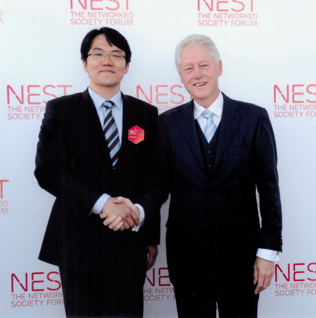


[ With President Bill Clinton at the Networked Society Forum in Hong Kong]
[ http://www.ericsson.com/nestforum/ ]

