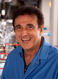
| Gregory J. Salamo Department of Physics (University of Arkansas, USA) | Solitons Optical Computing Optical Properties of Nano-Structures Electronic Properties of Nano-Structures Nano-Device Fabrication Lab Ferroelectrics, etc |

| Zhiming M. Wang (University of Electronic Science and Technology of China, China) (Institute of Semiconductor, Chinese Academy of Science, China) | Compound semiconductors, epitaxial crystal growth, molecular beam epitaxy (MBE), quantum dots, surface, interface, nanostructures, nanoscience and nanotechnology |

| James S. Harris Department of Electrical Engineering (Stanford University) | * Molecular Beam Epitaxy * Nanofabrication * Optoelectronics * Non-linear Optics * Single Electron Devices * Quantum Computing Research Group Home Page |

| Arthur C. Gossard Materials & Electrical & Computer Engineering (University of California, Santa Barbara) | Research involves growth of artificially structured materials by molecular beam epitaxy, including growth of quantum wells, superlattices and nanostructures, and their applications to high performance electrical and optical devices. Research Group Home Page |

| Pierre M. Petroff Materials Department (University of California, Santa Barbara) | * Self-assembled nanostructures using molecular beam epitaxy. * Self-assembled quantum wires and dots in III-V * compounds semiconductors. UCSB LINK |

| James S. Speck Materials Department (University of California, Santa Barbara) | Semiconductor research emphasizes relationships between thin film electronic materials growth, microstructure and physical properties. Experimental work focuses on MOCVD or MBE growth of wide bandgap nitrides coupled with structural characterization by transmission and scanning electron microscopy, x-ray diffraction, and atomic force microscopy. |
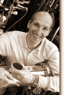
| Darrell G. Schlom Department of Materials Science and Engineering (Penn State University ) | Oxide Thin Films Electronic Materials Ferroelectrics Dielectrics Epitaxial Thin Films Molecular-Beam Epitaxy (MBE) Pulsed-Laser Deposition (PLD) Research Group Home Page |

| April Brown Electrical and Computer Engineering (Duke University) | III-V semiconductor materials and devices Control of nanostructure synthesis via strain and surface chemisry Heterojunction and Surface Engineering for Specific Device Applications and Defect Control GaAs-, InP-, GaSb-, and GaN- based materials Current Device Studies in AlGaAs-InAs High Electron Mobility Transistors, AlGaN UV Emitters, Integrated InP-based Heterojunction Bipolar Transistors Research Group Home Page |
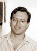
| Rod Beresford Professor of Engineering (Brown University) | Semiconductor nanostructures, including synthesis, modeling, integration with microelectronics, and applications Research Group Home Page |

| Haeyeon Yang Nano Science and Engineering (South Dakota School of Mines & Technology, USA) | Fabrication and syntheses of novel nano materials for optoelectronic devices including photovoltaics, light emitting diodes (LEDs) and lasers |

| Joanna Mirecki Millunchick Department of Materials Science & Engineering (University of Michigan) | Materials and surface sciences of semiconductor thin film nucleation and epitaxy Research Group Home Page |

| Rachel S. Goldman Materials Science & Engineering (University of Michigan) | Investigations of structure-property relationships in thin films and heterostructures. Of particular interest are the effects of strain relaxation (dislocations, surface and interface roughness), alloy formation (phase separation, clustering, ordering), and diffusion (and interdiffusion) on electronic and optical properties. Research Group Home Page |
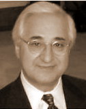
| Theodore Moustakas Electrical and Computer Engineering (Boston University) | Visible and UV LEDs: UV semiconductor lasers HVPE GaN templates Nitrogen cluster source: A-plane growth of GaN: Research Group Home Page |

| Ya-Hong Xie Department of Materials Science and Engineering (University of California, Los Angeles) | RF Cross-talk Isolation Self-assembled Quantum Dot Arrays by epitaxy Si Optical Bench Research Group Home Page |

| Christopher Palmstrøm Department of Chemical Engineering and Materials Science (University of Minnesota) | Epitaxial growth processes and heterostructure formation, Properties of thin films Research Group Home Page |
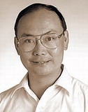
| Charles W. Tu Department of Electrical and Computer Engineering (University of California, San Diego) | * Arsenide/phosphide/nitride-based heterostructures and selective-area regrowth on patterned-and-etched substrates to improve device performance * A new class of semiconductors, dilute nitrides, for optoelectronic applications |
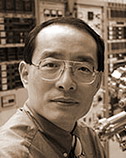
| Yong-Hang Zhang Electrical Engineering (Arizona State University) | Molecular beam epitaxy (MBE) Optoelectronic devices and their applications Research Group Link |
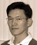
| Seongshik (Sean) Oh Department of Physics & Astronomy (Rutgers, the State University of New Jersey) | Atomically-controlled Oxide-Metamaterials Nano/micro Oxide Devices Research Group Home Page |

| Diana Huffaker Electrical Engineering (University of California, Los Angeles) | Directed and self-assembled nanostructure solid-state epitaxy, optoelectronic devices including solar cells and III-V/Si photonics |

| Pallab Bhattacharya Electrical Engineering and Computer Science (University of Michigan) | Bacteriorhodopsin-Semiconductor Biophotonic Integrated Circuits High Performance Quantum Dot Lasers and Photonic Circuits on Si CMOS Photonic Crystal Optical Microcavities Quantum Dot Infrared Photodetectors and Imaging Arrays Spin-Based Optoelectronics ZnO Growth by Plasma-Assisted Molecular Beam Epitaxy |

| William A Doolittle School of Electrical and Computer Engineering (Georgia Institute of Technology) | Wide bandgap semiconductor materials and devices Dielectric materials growth and characterization Electrical, optical and structural characterization and optimization of Electronic materials and devices Microelectronic device/circuit fabrication Radio frequency power electronic devices Research Group Link |

| John Prineas Department of Physics and Astronomy University of Iowa | Nonlinear optical materials for slowing, trapping, and switching optical pulses Mid- and long-wave optoelectronics (2-12 microns) and glucose sensing |

| Kang L. Wang Electrical Engineering (University of California, Los Angeles) | Nanoelectronics and optoelectronics, MBE and superlattices, micro-wave and millimeter electronics/optoelectronics, and quantum computing |

| Charles H. Ahn Department of Applied Physics (Yale University) | Novel materials; molecular beam epitaxy; physics and technology of ferroelectric films, including nanofabrication and “writing” with atomic force microscopy; control of carrier density in superconductors and semiconductors with ferroelectric gates Research Group Link |
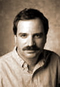
| Eric I. Altman Department of Chemical Engineering (Yale University) | Oxygen plasma molecular beam epitaxy system Dynamics of processes at surfaces using scanning tunneling microscopy (STM) and related techniques; structure-reactivity relationships in oxide catalysts; manipulation of surface chemistry through novel routes; the nucleation and growth of thin films |

| Victor E. Henrich Applied Physics and of Physics (Yale University) | Oxide MBE Solid surfaces, the interaction of surfaces with absorbed atoms and molecules, interfaces between solids, and the properties of complex oxides |

| Daniel Wasserman Department of Physics (University of Massachusetts Lowell) | mid-infrared (mid-IR) emitters, detectors, and photonic devices for applications in Medicine, the Environment, Homeland Defense, and Communications |

| William D. Goodhue Department of Physics (University of Massachusetts Lowell) Photonics Center Director | Experimental semiconductor research, materials, fabricatio |

| Manijeh Razeghi Electrical Engineering and Computer Science, (Northwestern University) | MBE & MOCVD Quantum optoelectronics Research Lab |

| Shuji Nakamura Materials Department (University of California, Santa Barbara, USA) | Nitride LED (blue laser LD and LED) The Solid State Lighting and Display Center at UCSB Dream of the Blue Laser Diode (I actually thought it looked very easy to make blue LEDs) |

| Jerry D. Tersoff (IBM Watson Research Center, USA) | Theoretical studies of self-assembly of epitaxial nanostructures |

| Dieter Bimberg (Technische Universitat Berlin, Germany) | Quantum Dots & QD laser |
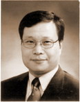
| Euijoon Yoon Department of Materials Science and Engineering (Seoul National University, South Korea) | III-V compound semiconductors Nitride QDs (MOCVD) Department of Materials Science and Engineering at Seoul National University |

| Alexander Govorov Department of Physics and Astronomy (Ohio University, USA) | Optics of quantum dots and rings Theoretical studies of photo-thermal effects in nanoparticle assemblies |

| Ho Nyung Lee (Oak Ridge National Laboratory, USA) | Functional Complex Oxides (PLD) |

| Christoph Lienau Institute of Physics (Carl von Ossietzky the University of Oldenburg, Germany) | Ultra fast Nano-Optics |

| Shu-Shen Li (Institute of Semiconductor CAS, China) | Theoretical studies of quantum- and nano-structures |

| Chih-Kang (Ken) Shih Department of Physics (University of Texas at Austin, USA) | Nano Electronic Materials Research Group Home Page |

| Oliver G. Schmidt (Max Planck Institute for Solid State Research, Germany) | Self-assembled quantum dots Free-standing nano-objects |
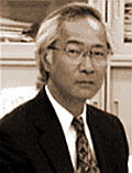
| Nobuyuki Koguchi (National Institute for Materials Science, Japan) | Droplet epitaxy |
Karl Jacobi (Fritz-Haber-Institut der Max-Planck-Gesellschaft, Germany) | High-index GaAs surfaces (MBE &STM) |

| David J. Smith Department of Physics ( Arizona State University, USA) | Tunneling Electron Microscopy (TEM) |
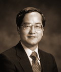
| Yasuhiko Arakawa (The University of Tokyo, Japan) | Quantum Dot Laser |

| Xiaoqin Li (Elaine) Department of Physics (University of Texas at Austin, USA) | Ultra fast nonlinear spectroscopy in condensed matter, quantum dynamics and control in nanostructures |

| Eric Stinaff Dept. of Physics & Astronomy (Ohio University, USA) | Optical and electronic properties of novel semiconductor materials, nanostructures and nanostructure based devices |

| Sophia E. Hayes Department of Chemistry (Washington University in St. Louis, USA) | Laser-Enhanced Solid-State Nuclear Magnetic Resonance |

| Roberto Morandotti (INRS EMT center University of Quebec, Canada) | Discrete optical solitons Ultra fast All-Optical Signal/Pulse Processing Ultra-Wide band (UWB) microwave signal processing Ultra fast Optical Processing Research Group |
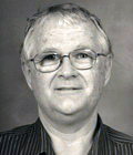
| George I. Stegeman College of Optics and Photonics (University of Central Florida, USA) | Nonlinear optics in waveguide structures: solitons in photonic crystals, in semiconductor optical amplifiers, in quasi-phase-matched doubling crystals and in the discrete systems Soliton group |

| Arup Neogi Department of Physics (University of North Texas, USA) | – Ultra fast and nonlinear optical effects in nitride semiconductors, intra-sub-band device physics, organic- inorganic luminescent hetrostructure and optical sensing and bio-imaging using semiconductor quantum dots |

| Brian P. Gorman Department of Materials Science and Engineering (University of North Texas, USA) | – Nanostructured inorganic materials processing and characterization with a thin film emphasis – Characterization of thin films and ceramic interfaces using HRSTEM, TED,FESEM, XRD, and optical techniques – Low temperature processing of nanoscale fuel cells, low-k dielectrics, and optoelectronics using precursor, sol-gel, and colloidal depositions – Interfacial studies, epitaxial growth, texturing, and grain growth in thin films |

| Maohai Xie Department of Physics (The University of Hong Kong, Hong Kong) | – Surface Science: Molecular Beam Epitaxy, Growth Kinetics, Semiconductor Surface Structures Department directory link |
| Tae-Youl Choi Department of Mechanical and Energy Engineering (University of North Texas, USA) | – Nanostructure characterization/Fabrication of nanowire sensors – Femtosecond laser material processing – Focused ion beam nanofabrication |

| Littler Department of Physics (University of North Texas, USA) | Eletrical and optical characterization of novel semiconductor materials |

| Michael Shur | – Semiconductor Materials and Devices (nitride) SiC and Related Materials and Devices by Michael Shur |

| Shriram Ramanathan Materials Science (Harvad University) | – Mechanistic understanding of role of electric fields in initial oxidation kinetics of metals and alloys – Size effects on ion conduction mechanisms in doped-fluorite oxides – Phase transition mechanisms in rutile oxides and their active tuning – Precise measurements of oxygen concentration and migration kinetics at oxide hetero-interfaces |

| Eugene A. Fitzgerald Department of Materials Science Engineering (Massachusetts Institute of Technology) | Materials Science Engineering (Massachusetts Institute of Technology) Prof. Fitzgerald’s group’s research activities attack the current limitations of electronic materials, especially limitations created by imperfections in materials such as point, line, and planar defects. Much of the group’s efforts are focused on lattice-mismatched semiconductor systems, in which layers in electronic materials and devices have different lattice parameters. Prof. Fitzgerald’s Home |

| Xiang Zhang Department of Mechanical Engineering (University of California at Berkeley) | Micro-nano scale engineering, novel 3D fabrication technologies in microelectronics and photonics, micro and nano-devices, nano-lithography and nano-instrumentation, rapid prototyping, bio-MEMS, and semiconductor manufacturing. |

| Jin Kyu Lee School of Chemistry and Molecular Engineering (Seoul National university) | Organic-inorganic Nanocomposite |

| Zhong Lin (ZL) Wang School of Materials Science and Engineering (Georgia Institute of Technology) | 1. Nanowires and nanobelts of semiconducting oxide: from materials, to properties and to devices (2000 – present). 2. In-situ nanomeasurements on the mechanical, electrical and field emission properties of nanostructures (1997 – present). 3. Dynamics of shape controlled nanocrystals and nanocrystals self-assembly (1995 – present). |

| Wonbong Choi Department of Mechanical and Materials Engineering (Florida International University) | Nanotube/ Nanowire growth Nanoelectronics Field emission Nano Biosensors |

| Samuel S. Mao Department of Mechanical Engineering (University of California at Berkeley) | Energy transport, conversion and storage, Nano, micro and meso scale phenomena and devices, Ultrafast laser-material interactions, Materials processing, Nonlinear science. |
| Lionel C. Kimerling Department of Materials Science Engineering (Massachusetts Institute of Technology) | Materials processing and device engineering for the creation of micron and sub-micron scale device elements for vertical integration with circuit systems. |

| Steven P. DenBaars Materials & Electrical & Computer Engineering (University of California, Santa Barbara) | Electronic Materials growth and fabrication of new semiconductor devices. MOCVD of III-V compound semiconductor materials and devices (InP, GaN). Special interests include the effect of materials properties on device performance Blue LEDs, Blue Lasers, and High Temperature, High Power Electronic Devices. Research Group Link |

| Mark A. Reed Engineering and Applied Science (Yale University) | Heterojunction and low dimensional device physics; mesoscopic physics; quantum devices; nanotechnology; molecular scale transport; plasmonics; nanoscale biosensors Research Group Link |

| Robert J. Schoelkopf Applied Physics and Physics (Yale University) | Quantum transport, single-electron devices, and charge dynamics in nanostructures. Broadly put, his research is concerned with quantum-effect and single-electron devices |

| Jung Han Electrical Engineering (Yale University) | Organo-metallic vapor phase epitaxy (OMVPE) AlGaInN blue and ultraviolet light emitting diodes (LEDs) and laser diodes (LDs) III-Nitride vertical cavity surface emitting lasers and LEDs GaN and AlGaN Quantum Dots through Droplet Epitaxy |

| Hyatt M. Gibbs Optical Sciences (The University of Arizona) | Fundamental physics of semiconductor quantum-confined structures; nonlinear optical phenomena; molecular-beam-epitaxial growth of Ga,Al,ln,As heterostructures; vertical-cavity surface-emitting lasers; optical instabilities; nonlinear etalons and waveguides; optical nonlinearities. Research Lab |
